Авторизация
Сейчас на сайте
Счетчики
Bakomchev's designs - amplifiers, indicators, triggers ...
Bakomchev's designs - amplifiers, indicators, triggers ...
One-stage amplifier of the frequency converter (Fig. 1)
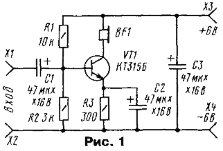
This is the simplest design that allows you to demonstrate the amplifying capabilities of a transistor. True, the voltage gain is small - it does not exceed 6, so the scope of such a device is limited. Nevertheless, it can be connected, say, to a detector radio (it must be loaded with a 10 kΩ resistor) and use the BF1 headphone to listen to the broadcasts of a local radio station.
The amplified signal is supplied to the input sockets X1, X2, and the supply voltage (as in all other constructions of this author, it is 6 V - four galvanic cells with a voltage of 1.5 V connected in series) are supplied to the sockets X3, X4. The divider R1 R2 sets the bias voltage at the base of the transistor, and the resistor R3 provides current feedback, which contributes to the temperature stabilization of the amplifier.
How does stabilization work? Suppose that under the influence of temperature the collector current of the transistor increased. Accordingly, the voltage drop across the resistor R3 will increase. As a result, the emitter current decreases, and hence the collector current - it reaches the initial value.
The load of the amplifier stage is a headphone with a resistance of 60 ... 100 Ohms.
It is not difficult to check the operation of the amplifier, you need to touch the input socket X1, for example, with tweezers - a weak buzzing should be heard in the phone, as a result of AC pickup. The collector current of the transistor is about 3 mA.
Two-stage amplifier of the frequency converter on transistors of different structures (Fig. 2)
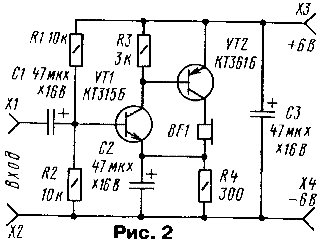
It is made with a direct connection between the cascades and deep negative direct current feedback, which makes its mode independent of the ambient temperature. The basis for temperature stabilization is resistor R4, which "works" similarly to resistor R3 in the previous design.
The amplifier is more "sensitive" compared to a single-stage amplifier - the voltage gain reaches 20. The input jacks can be supplied with alternating voltage with an amplitude of not more than 30 mV, otherwise there will be distortions heard on the headset.
Check the amplifier by touching the tweezers (or just a finger) of the input jack X1 - the phone will sound loud. The amplifier consumes current of about 8 mA.
This design can be used to amplify weak signals, for example, from a microphone. And of course, it will significantly enhance the RF signal removed from the load of the detector receiver.
Two-stage amplifier of the frequency converter on transistors of the same structure (Fig. 3)
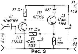
A direct connection between the cascades was also used here, but the stabilization of the operating mode is somewhat different from previous designs. Assume that the collector current of the transistor VT1 has decreased. The voltage drop across this transistor will increase, which will lead to an increase in voltage across the resistor R3 included in the emitter circuit of the transistor VT2. Due to the connection of transistors through resistor R2, the base current of the input transistor will increase, which will lead to an increase in its collector current. As a result, the initial change in the collector current of this transistor will be compensated.
The sensitivity of the amplifier is very high - the gain reaches 100. The gain largely depends on the capacitance of the capacitor C2 - if you turn it off, the gain will decrease. Input voltage should be no more than 2 mV.
The amplifier works well with a detector receiver, with an electret microphone and other sources of weak signal. The current consumed by the amplifier is about 2 mA.
Two-stroke power amplifier for the AF (Fig. 4)
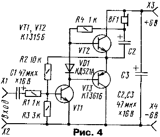
It is made on transistors of different structures and has a voltage gain of about 10. The highest input voltage can be 0.1 V.
The amplifier is two-stage: the first is assembled on a transistor VT1, the second - on VT2 and VT3 of a different structure. The first stage amplifies the AF signal by voltage, and both half-waves are the same. The second one amplifies the current signal, but the cascade on the transistor VT2 "works" with positive half-waves, and on the transistor VT3 - with negative.
The constant current mode is chosen so that the voltage at the junction point of the transistor emitters of the second stage is approximately half the voltage of the power source. This is achieved by turning on the feedback resistor R2. The collector current of the input transistor, flowing through the VD1 diode, leads to a voltage drop on it, which is the bias voltage at the bases of the output transistors (relative to their emitters) - it allows you to reduce the distortion of the amplified signal.
The load (several headphones connected in parallel or a dynamic head) is connected to the amplifier through an oxide capacitor C2. If the amplifier will work on a dynamic head (with a resistance of 8 ... 10 Ohms), the capacitance of this capacitor should be at least twice as large.
Pay attention to the load connection of the first stage - resistor R4. Its top terminal in the circuit is connected not with the power plus, as is usually done, but with the lower terminal of the load.
This is the so-called boost circuit, in which a small voltage of positive feedback is applied to the base circuit of the output transistors, equalizing the operating conditions of the transistors.
Two-level voltage indicator (Fig. 5)
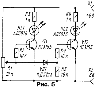
Such a device can be used, for example, to indicate "depletion" of the power battery or to indicate the level of the reproduced signal in a household tape recorder. The indicator layout allows you to demonstrate the principle of its operation.
In the lower position of the engine of the variable resistor R1, both transistors are closed, the LEDs HL1, HL2 are off. When you move the resistor slider up, the voltage on it increases. When it reaches the opening voltage of transistor VT1, LED HL1 will flash.
If you continue to move the engine, there will come a moment when, following the diode VD1, the transistor VT2 opens. The HL2 LED will also flash. In other words, a low voltage at the input of the indicator causes only the HL1 LED to glow, and a larger one - both LEDs.
By smoothly reducing the input voltage with an alternating resistor, we notice that first the HL2 LED goes out, and then the HL1 LED goes out. The brightness of the LEDs depends on the limiting resistors R3 and R6: when their resistance increases, the brightness decreases.
To connect the indicator to a real device, you need to disconnect the top output of the variable resistor from the plus wire of the power source and apply a controlled voltage to the extreme terminals of this resistor. By moving its engine, the threshold for “triggering” the indicator is selected.
When monitoring only the voltage of the power supply, it is permissible to install a green LED (AL307G) in place of HL2.
Three-level voltage indicator (Fig. 6)
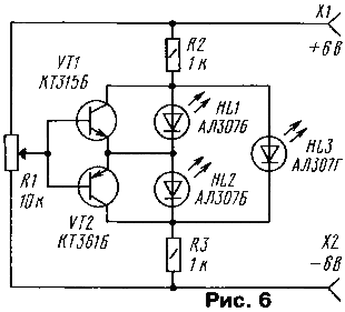
It gives out light signals according to the principle less than the norm - the norm is more than the norm. For this, two red LEDs and one green LED are used in the indicator.
At some voltage on the engine of the variable resistor R1 (“voltage is normal”), both transistors are closed and only the green LED HL3 “works”. Moving the resistor slider up in the circuit leads to an increase in voltage (“above normal”) on it. The transistor VT1 opens. The HL3 LED goes out, and the HL1 lights up. If the engine is moved down and thus reduced voltage on it ("less than normal"), the transistor VT1 closes, and VT2 opens. The following picture will be observed: at first the LED HL1 will go out, then the HL3 will light up and soon go out, and finally HL2 will flash.
Due to the low sensitivity of the indicator, a smooth transition is obtained from the extinction of one LED to the ignition of another: it has not yet completely gone out, for example, HL1, but HL3 is already lit.
Schmitt trigger (Fig. 7)
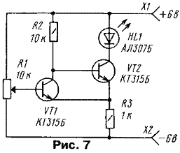
As you know, this device is usually used to convert a slowly changing voltage into a square wave signal.
When the variable resistor R1 slider is in the lowest position in the circuit, the transistor VT1 is closed. The voltage on his collector is high. As a result, the transistor VT2 is open, which means that the LED HL1 is lit. A voltage drop forms on resistor R3.
Slowly moving the variable resistor slider up in the circuit, it will be possible to reach the moment when the transistor VT1 jumps open and VT2 closes. This will happen when the voltage drop on the base of VT1 exceeds the voltage across resistor R3. The LED will turn off.
If after that you move the engine down, the trigger will return to its original position - the LED will flash. This will happen when the voltage on the engine is less than the voltage off the LED.
Source: Radio No. 6, 2000 by RADIUS.kz


Letzte Kommentare
Artikel
Fotos
Eigene Seiten